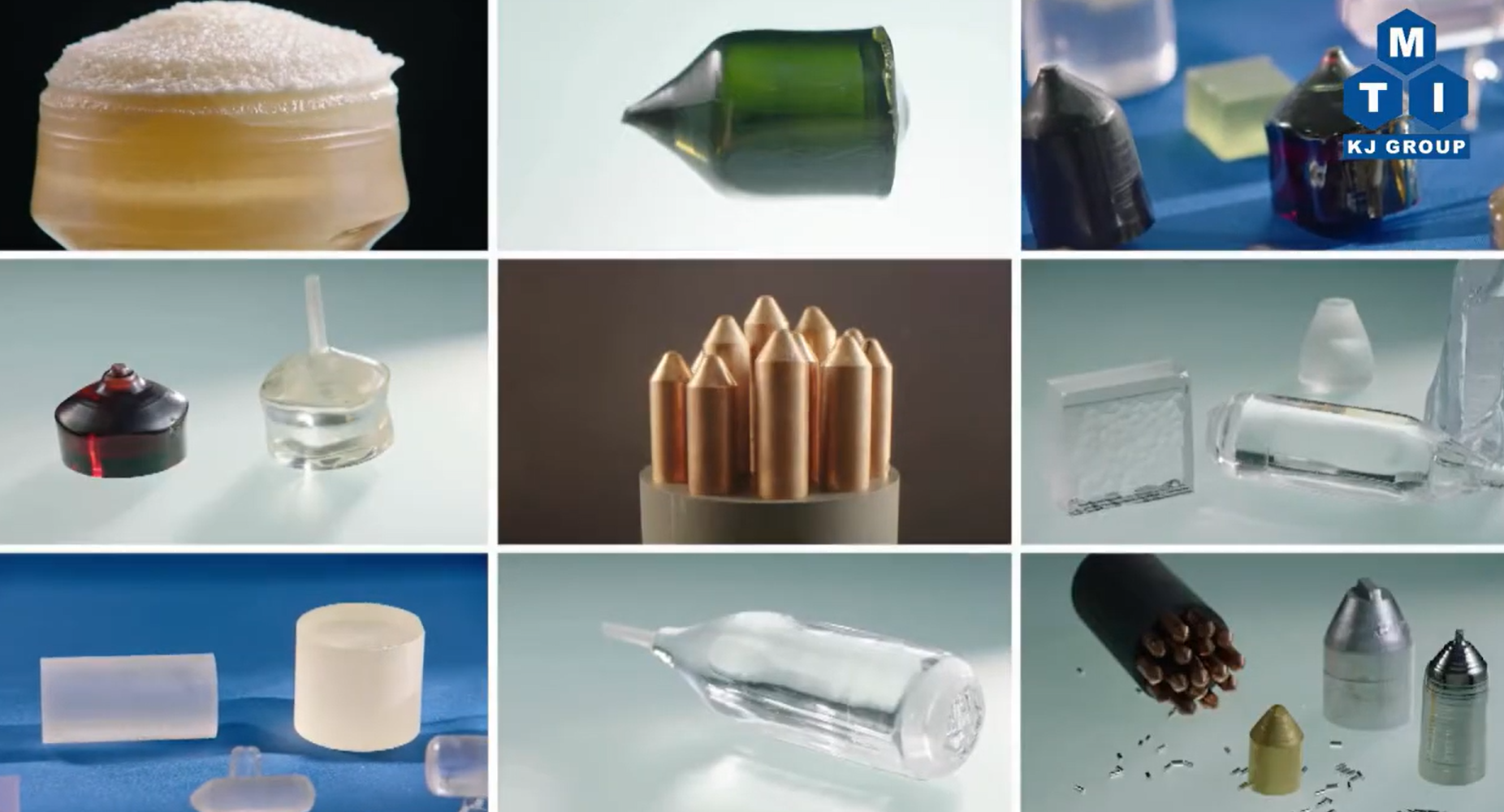
MTI Corporation offers a wide selection of high-quality crystalline materials supporting research in microelectronics, photonics, quantum technologies, and energy systems.
The portfolio includes semiconductors, conductors, insulating and optical materials, all selected for their structural integrity, purity, and consistency.
This diversity enables a broad range of electrical, optical, thermal, and mechanical properties required for advanced scientific research and device development.
Available Materials & Substrates
We provide a comprehensive range of materials for both research and industrial applications:
Metals (Elements)
Ag, Al, Au, Co, Cr, Cu, Fe, Hf, In, Li, Mg, Mo, Ni, Pb, Pd, Ti, V, W, Zn, Zr
Alloys
• Fe–Co–Ni Alloy
• SS-316 (Stainless Steel)
Semiconductors
• Si, Ge
• GaAs, GaN, GaP, GaSb
• InAs, InP, InSb
• SiC (4H, 6H, 3C)
• Ga₂O₃
Oxides (Ceramics & Crystals)
• Al₂O₃ (Sapphire), MgO, SrTiO₃
• TiO₂ (Rutile / Anatase), YSZ
• CeO₂, NdGaO₃, LaAlO₃, LSAT, ZnO
Nitrides
• AlN, Si₃N₄, hBN
Fluorides & Halides
• CaF₂, BaF₂, MgF₂, LiF
• NaCl, KCl, LaF₃
Carbon-Based Materials
• Graphite, Pyrolytic Graphite
• Diamond, Diamond on Si
• Carbon Substrate & Foam
Optical & Scintillator Crystals
• BGO, CsI(Tl)
• YAG, YVO₄, YIG
• Lu₂SiO₅, PbWO₄, CdWO₄
2D Materials
• MoS₂, MoSe₂, MoTe₂
• WS₂, WSe₂, WTe₂
• Black Phosphorus
Specialized / Engineered Substrates
• SOI, SOS
• Glass, Quartz (SiO₂), Mica
• BeO, SiC ceramics
• Conductive ceramics, TiO₂, ZnO substrates
Available Forms
- Bulk materials
- Wafers / Substrates
- Epitaxial films / Coated substrates
- Foils & foam sheets
- Disks and custom shapes
Specifications & Customization
We support fully tailored solutions:
• Wide range of dimensions and thicknesses
• Defined crystallographic orientations (e.g. (100), (110), (111))
• Surface finishes: SSP / DSP
• Doping and epitaxial layers on request
• Optical / epi-ready surface quality
• Tight control on thickness and flatness
• Custom geometries and small-quantity supply
Typical Application Example
A representative product in our portfolio is the GaAs single crystal wafer, widely used in high-frequency electronics and optoelectronic device research.
GaAs Single Crystal Wafer
• Growing method: VGF
• Orientation: (110)
• Size: 2″ diameter × 0.5 mm thickness
• Polishing: Double-side polished (DSP)
• Doping: Undoped
• Conductivity type: Semi-insulating (SI)
• Carrier concentration: N/A
• Mobility: 3710–6230 cm²/V·s
• EPD: N/A
• Resistivity: (0.8–4.8) × 10⁸ Ω·cm
• Surface roughness (Ra): < 0.4 nm
• Surface condition: EPI-ready
• Packing: Standard clean packaging
This type of wafer is commonly used in microwave devices, RF components, and advanced semiconductor research due to its high resistivity, low surface roughness, and excellent electronic transport properties.
Contact
Feel free to contact us to discuss your specific material requirements. Our team will be glad to support your project with tailored solutions.
contact@accessr-energy.eu